搜索

 电子科学与技术教研室(电子工程系)
 职称:教授 博导
 职务:信息学院教授委员会成员
 电子邮件:yifangchen@fudan.edu.cn
 办公地点:上海市复旦大学江湾校区叉二楼B7011室
 电话:0086-021-55664054
 课题组主页:
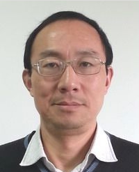
一、纳米光刻与纳米工艺技术
1. 高分辨率电子束光刻(High resolution electron beam lithography)
2. 三维灰度电子束光刻技术(Greyscale electron beam lithography for 3D profile)
3. 纳米压印光刻(Nanoimprint lithography)
4. 泰伯效应纳米光刻(Talbot nanolithography)
5. 纳米尺度反应离子刻蚀(Nanoscale reactive ion etch)
6. 深硅电感耦合反应离子刻蚀(Deep silicon reactive ion etch by inductively coupled process)
7. 纳米尺度金属电镀(Nanoscale metal electroplating)
二、微纳工艺与纳米制备(Micro nano processing & nanofabrications):
1. 同步辐射X射线光学系统关键部件(菲涅尔波带片,汇聚透镜,光栅,分辨率测试卡,光束阻挡器,光阑)(Optical components in synchrotron radiation X ray optical system)
2. 纳米压印模板(NIL templates/stamps/shims)
3. 氮化硅隔膜技术(SiNx membrane technique)
4. 硅基隔膜技术 (Si membrane technique)
5. 各种微纳尺度的纳米结构与器件(Various nanostructures and nanodevices)
三、纳米电子器件和新型红外光电探测器(Nanoelectronic devices and infrared photoelectronic devices)
1.高电子迁移率晶体管和T形栅(High electron mobility transistors (HEMTs) and T gates) 2. 低维系统量子输运系统(Quantum transport in lower dimensional systems:2DEG, 1DEG, 0DEG quantum dots)
3. 短波红外偏振探测器和芯片(Polarization detectors and chips in short infrared wavelengths)
4. 全硅基短波红外光电探测器与焦平面芯片 (Si based photoelectronic detectors and focal plane chips in short infrared wavelengths)
四、纳米光子学与超表面材料(Nanophotonics & metasurface)
1. 二维纳米光子晶体和超表面材料的加工与光学特性研究(Fabrications and optical properties of 2D nanophotonics & metasurfaces)
2. 纳米结构色(Coloring effects by nanophotonic structures and metasurfaces)
3. 涡旋光场的相位调制板技术(Optical vortex by phase modulation plate technique)
4. 纳米仿生结构(Nanobionic structure: technology, science and applications )
4.1 自然生物结构的纳米制备(Nanofabrications of naturally occurring biological nanostructures)
4.2 自然仿生结构的光学物理特性研究(Optical and physical property study of fabricated nanobionic structures)