
Prof. Zhang Shuyu and his team demonstrated the ultra-wide processing window of antisolvent-assisted perovskite film preparation
Recently, Shuyu Zhang, associate professor of the Institute of Electric Light Sources, School of Information Science and Technology, Fudan University, and his group demonstrated the ultra-wide processing window of antisolvent-assisted perovskite film preparation with rare earth doping. On March 10th, the result was published on Advanced Electronic Materials with the title "Trivalent-Neodymium Additive Modulated MAPbBr3 Perovskite Nucleation and Growth: Ultrawide Processing Window for One-step Fabrication of Efficient Light-Emitting Perovskites", and was selected as the inside back cover.
Figure 1. Inside Back Cover of Advanced Electronic Materials (March 2020)
Hybrid metal halide perovskite-based LEDs and lasers have demonstrated outstanding performance and are currently leading a new trend in the optoelectronic field. However, the widely used one-step spin-coating method assisted by an antisolvent suffers from the narrow processing window of antisolvents, which limits its further use in commercial applications. To address this issue, Zhang’s group demonstrated a solution of incorporating Nd3+ into MAPbBr3 nanocrystals, and achieved an ultrawide processing window of 18 s, which is significantly larger than the traditional time window of 3-5 s.
The Nd3+ doping can effectively improve the crystallinity, suppress Pb atoms and reduce defects and pinholes, therefore contributing to a 6-fold enhancement of film PLQY and an excellent stability of 8 months in ambient conditions. This strategy paves the way towards large-scale production of perovskite thin films with higher yield and better stability.
Zhang’s group also analyzed the doping mechanism, revealing that the Nd3+ induced heterogeneous nucleation leads to improved crystallization of MAPbBr3 and contributes to the ultra-wide process window, which provides a new perspective for the study of rare earth doped perovskites.
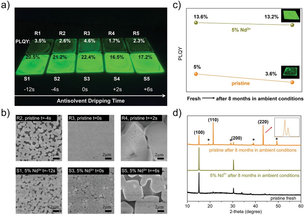
Figure 2. a) Photograph of pristine MAPbBr3 thin films (first row) and MAPbBr3:Nd(5%) thin films (second row) with different antisolvent dripping time, marked as R1–R5 and S1–S5. b) SEM images of samples R2, R3, R4, S1, S3, and S5. Stability of pristine and MAPbBr3:Nd(5%) thin films: c) PLQY and photograph, and d) XRD patterns, where the inset shows the magnified (220) peak of pristine films stored for 8 months.
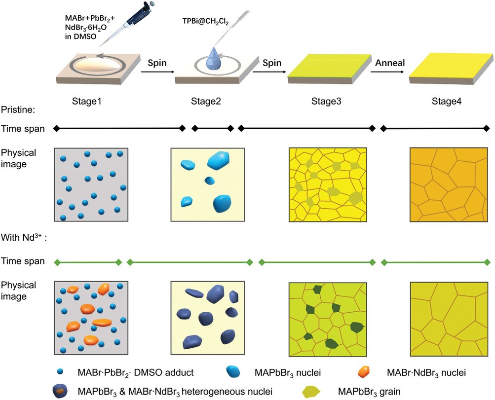
Figure 3. Schematic illustration of the four stages in the one-step spin-coating process assisted by an antisolvent. The time span was experimentally observed, and images of the nucleus formation and crystal growth help depict the physical process, in accordance with the broadening of processing window and other phenomena.
This work is supported by the National Natural Science Foundation of China (61705042, 51677031, 11975081), Shanghai Sailing Program (16YF1400700), Shanghai Science and Technology Committee (18JC1411500), and National Key Research and Development Program of China (2017YFB0403603).