
Breakthroughs in novel semiconductor photodetector and image sensor by Prof. Wan Jing’s group
Recently, Prof. Wan Jing’s group from the School of Information Science and Technology at Fudan University has made several breakthroughs in the research of novel semiconductor photodetector and image sensor. These breakthroughs have been published in Advanced Functional Materials (IF: 15.6; 10.1002/adfm.201906242), and IEEE Electron Device Letters (10.1109/LED.2019.2892782 and 10.1109/LED.2019.2908632).
Wavelength Photodetector:
Prof. Wan Jing and Prof. Bao Wenzhong from the School of Microelectronic Engineering (MEE) have cooperated to combine novel device physics and 2D materials, and invented several novel photodetectors.
Conventional photodetector is sensitive to the light intensity, where its output current or voltage is modulated by the light intensity. Jing proposed a photodetector controlled by multiple photogates. By combining the multiple photogates and novel 2D materials, a novel photodetector which is only sensitive to the wavelength has been demonstrated experimentally, see Fig. 1(a) and (b).
The result has been published in Advanced Functional Materials. Thanks to its unique property, the device can find applications in light spectrum scope, calibration of laser wavelength, detection of fluorescence and fire temperature meter.
Besides, Prof. Wan has invented interface coupled photodetector (ICPD), which, for the first time, utilizes the interface coupling effect in the silicon-on-insulator (SOI) substrate to augment the photodetection responsivity. This effect is further demonstrated with SOI/MoS2 heterojunction devices which shows tunable response spectrum, see Fig. 1(c) and (d). This result has been published in IEEE Electron Device Letters and can be potentially applied in multi-spectral image sensing.
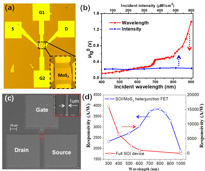
Fig. 1 (a) Novel wavelength photodetector and (b) its response to light with various wavelength and intensity;(c) interface coupled photodetector and its (d) response spectrum
Photoelectron in-situ sensing device (PISD) as a one-transistor active pixel sensor:
The core of the conventional CMOS image sensor is the CMOS active pixel sensor (APS). In order to achieve the functionalities, such as photosensing, charge integration, signal amplification and random access, the conventional CMOS APS needs to combine at least three transistors and one photodiode in a pixel cell.
This largely complicates its structural design and reduces the quantum efficiency. Jing discovered a unique deep depletion effect in the SOI substrate and utilized it for photosensing, which leads to the invention of photoelectron in-situ sensing device (PISD).
Jing’s cooperation with Prof. Jiang Yulong from the School of MEE has further improved this device with advanced CMOS technology, as shown in Fig. 2(a) and (b). Selected as the cover page of IEEE Electron Device Letters, see Fig. 2(c), the research is commented as “revolutionary” by its reviewer.
PISD, as a one-transistor APS (1T-APS), successfully combines all functionalities in one transistor. This can largely simplify the pixel design and improve its efficiency. Considering the huge market of image sensor, the development of PISD is very helpful for China to break the monopoly in the global market.
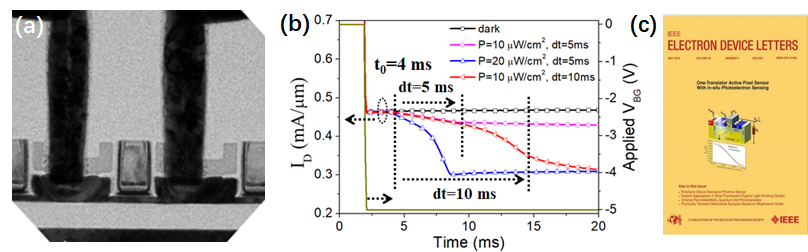
Fig. 2 (a)photoelectron insitu sensing device and (b)its response to various light pulses;(c) Cover page of IEEE Electron Device Letters with PISD